

New HBF spec outlines tech that can give GPUs terabytes of extra memory — Sandisk and SK hynix unveil spec with up to 16-Hi NAND stacks, 3 TB/s bandwidth, UCIe

Sandisk and SK hynix on Tuesday formally introduced the High Bandwidth Flash (HBF) specification, their jointly developed storage technology that promises to bring together the non-volatility of 3D NAND and the performance of High Bandwidth Memory (HBM), which will be handy for AI inference systems. The specification was released through the Open Compute Project (OCP), so it will be an open standard rather than a proprietary interface.
Tom’s Hardware Premium Roadmaps
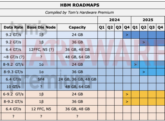
The initial specification defines HBF packages with capacities of up to 512GB using either 8-Hi or 16-Hi NAND die stacks, though these will not be standard 3D NAND stacks, but rather specialized devices with a fast interface. In fact, Sandisk once called them HBF core dies rather than 3D NAND die stacks.
Performance of HBF is divided into three bandwidth grades ranging from approximately 0.4 TB/s to 3.0 TB/s (though we are not sure whether this figure describes the full HBF subsystem or per-package bandwidth). Such a huge performance range implies that Sandisk and SK hynix expect HBF to have a multi-year roadmap featuring multiple implementations and generations of HBF. It is noteworthy that the most capable implementation of HBF (3 TB/s) is set to beat the memory bandwidth of a single HBM4 memory stack (2 TB/s), though it will be unlikely to beat HBM4 when it comes to latency.
Latest Videos FromTom’s Hardware
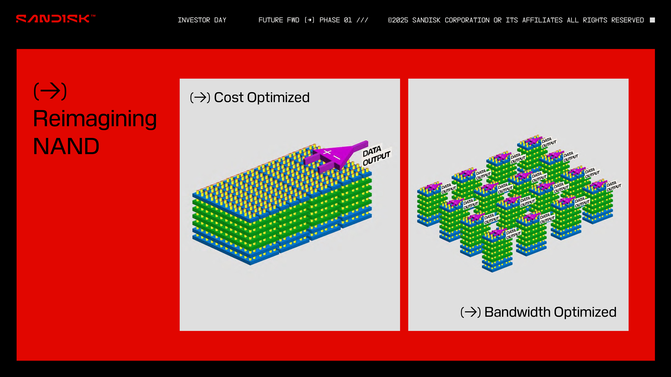
Interestingly, SK hynix claims that HBF uses the Universal Chiplet Interconnect Express (UCIe) standard to simplify integration with heterogeneous computing platforms, whereas Sandisk claims that HBF is set to adopt the ‘xPU-HBF’ interface, which could be its definition of UCIe implemented by companies like Broadcom or Marvell.
In addition to capacity and performance targets, the specification establishes electrical and interface characteristics, packaging and reliability guidelines for stacked HBF devices, as well as software I/O requirements. For now, these specifications are not officially published by the OCP.
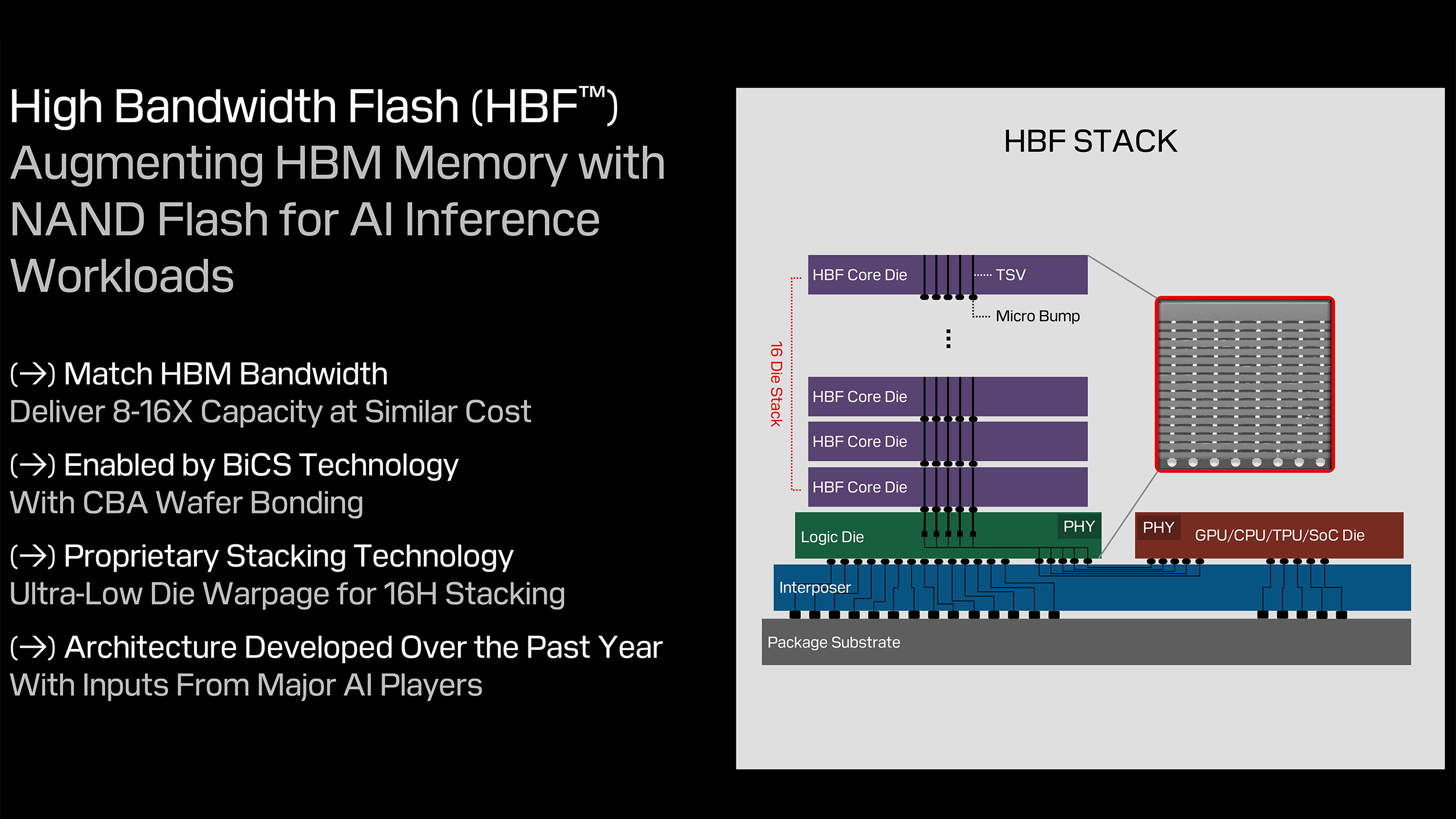
Extracting 400 GB/s of bandwidth from a single 512GB HBF package is not a trivial task. To enable such a package, Sandisk once planned to use 16 HBF core dies that feature many, many arrays that can be accessed concurrently using dedicated read/write paths. Meanwhile, it is possible to reach over 400 GB/s of bandwidth per package using a single UCIe interface that runs at up to 64 GT/s and features 64 lanes. Yet, this means that the HBF base die will be a fairly complex piece of silicon.
Sandisk and SK hynix position HBF as a new memory tier for AI inference workloads by combining near-memory bandwidth with the higher capacity and non-volatility of NAND flash. The technology is aimed at workloads that require substantially larger memory pools close to compute than HBM alone can economically provide. For example, while the maximum capacity of an HBM4 stack is 64GB, an HBF stack can provide up to 512GB. Even at a lower bandwidth, such memory can be useful for inference workloads.
Arguably the biggest question about HBF is who is going to adopt the technology? Since Sandisk and SK hynix announced plans to collaborate on defining the HBF specification in 2025, only Google and Tenstorrent have expressed interest in participating in the HBF consortium. Meanwhile, AMD, Broadcom, Intel, Nvidia, Marvell, Micron, Qualcomm, Samsung, and Western Digital have so far expressed no interest in HBF.

Follow Tom’s Hardware on Google News, or add us as a preferred source, to get our latest news, analysis, & reviews in your feeds.