

Hot Chips 2026: Fujitsu’s Monaka CPU stacks its entire cache on a separate 5nm die and narrows to 256-bit SVE2 — 350W and 500W SKUs due in 2027

This Tom’s Hardware Premium article is free to read with a Tom’s Hardware account; no payment necessary. We’re offering free access from August 23 to 26 so you can read all of our reporting from Hot Chips.
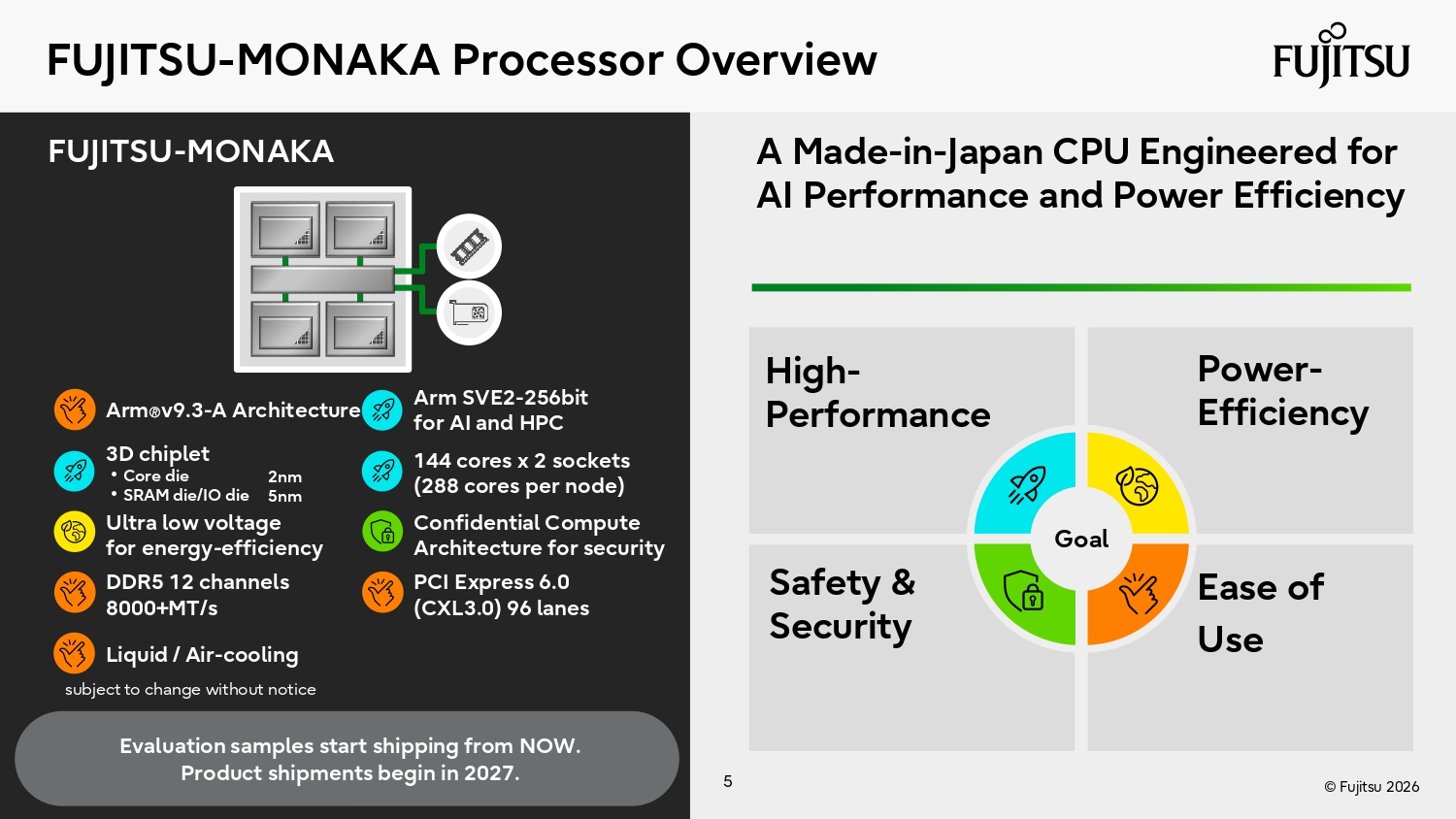
Fujitsu gave us a detailed look at its 144-core Monaka server CPU at Hot Chips 2026 on August 24, confirming for the first time that the Arm chip runs dual 256-bit SVE2 vector units, down from the 512-bit SVE in its A64FX predecessor, and that its entire last-level cache sits on a separate 5nm die beneath the 2nm compute die.
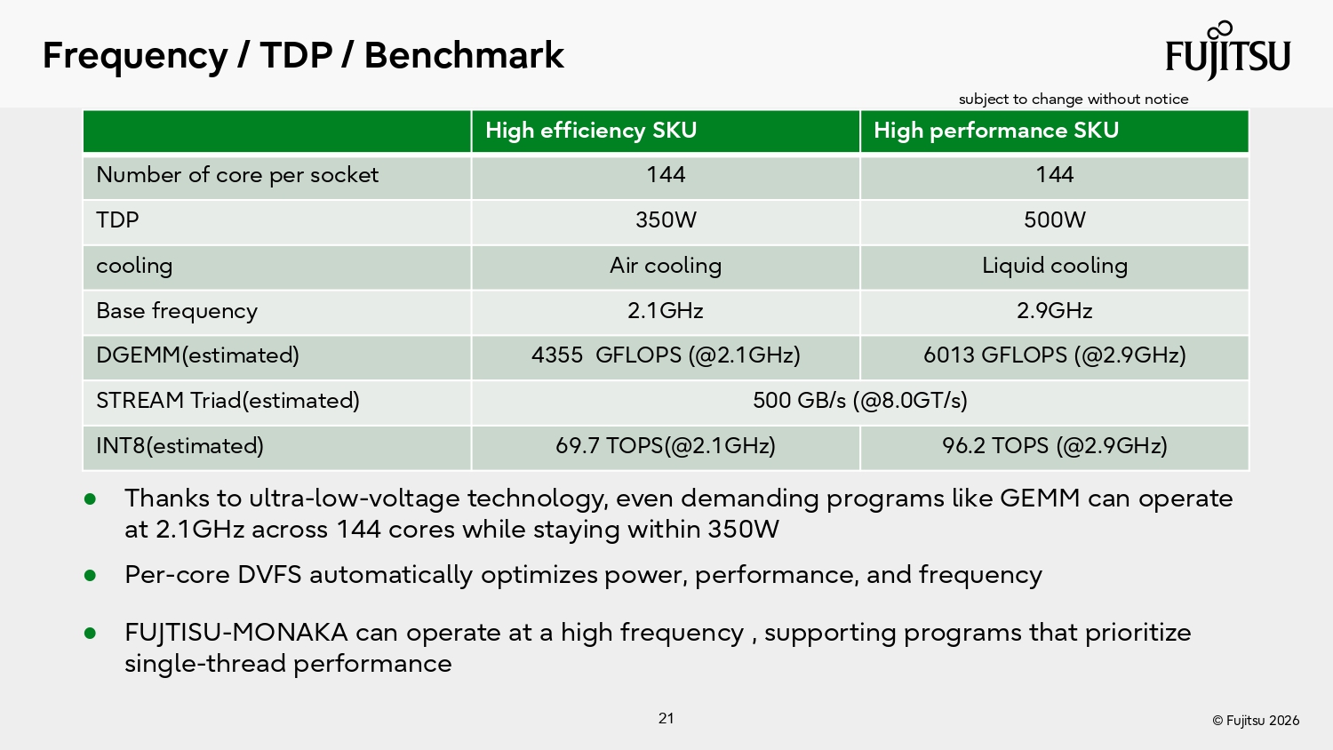
Ryohei Okazaki, lead architect of Fujitsu’s processor development team, presented the design as “a made-in-Japan CPU, specifically engineered for AI performance and power efficiency,” built for what the company calls green AI data centers and subsidized by Japan’s New Energy and Industrial Technology Development Organization. The chip ships in two SKUs: a 350W air-cooled part at 2.1 GHz base and a 500W liquid-cooled part at 2.9 GHz base, with evaluation samples available now and volume production in 2027.
Three dies, one stack
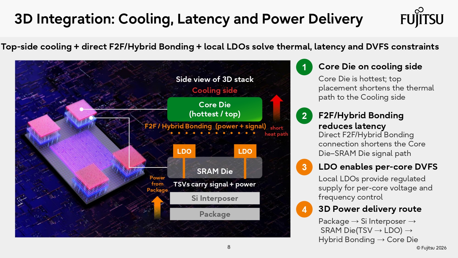
Monaka splits into three tiers of silicon: a 2nm core die on TSMC N2P, a 5nm SRAM die on TSMC N5 that holds the whole last-level cache, and a 5nm IO die. The core die stacks face-to-face on top of the SRAM die through hybrid bonding, sitting on the cooling side because it runs hottest, while the IO die connects to the SRAM die across a silicon interposer. Fujitsu keeps 2nm silicon under 30% of total die area, a split Okazaki said lets Fujitsu “accelerate the time to market for our 2-nanometer-based chip” by pushing everything that shrinks poorly onto the 5nm SRAM and IO dies.
Latest Videos FromTom’s Hardware
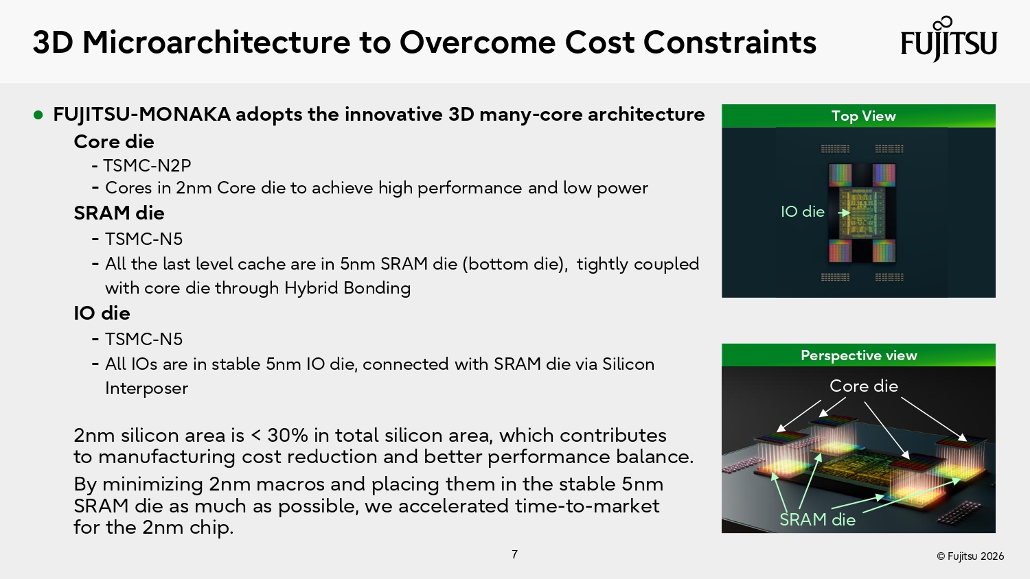
Putting the full last-level cache on a distinct stacked die separates Monaka from AMD’s 3D V-Cache, which bonds extra SRAM on top of a compute die that already carries its own L3, and lines it up closer to Intel’s Clearwater Forest, where local cache sits in a base tile with compute stacked above. Fujitsu also moved the low-dropout voltage regulators onto the 5nm SRAM die because analog circuits scale poorly at 2nm, and placed them directly beneath the core’s floating-point units to feed per-core dynamic voltage and frequency scaling.
Dr. Ian Cutress of More Than Moore asked whether Fujitsu was “doing anything special to minimize core-to-core latency” given that the core dies sit on opposite sides of the package and traffic routes through the IO die and back. Fujitsu pointed to the face-to-face hybrid bonding between the core and SRAM dies but declined to disclose latency figures.
From 512-bit vectors to 256
Chester Lam of Chips and Cheese asked why Fujitsu narrowed the vector datapath from the 512-bit SVE in A64FX to 256-bit SVE2 in Monaka. Okazaki said the chip is built “for [the] data center” and that Fujitsu wanted to “minimize the core size” for the best cost and performance, with the narrower units also cutting SIMD width for general-purpose code.
A64FX, the 7nm CPU that powered the Fugaku supercomputer and became the first chip to implement Arm SVE, paired its 512-bit vectors with on-package HBM2 for memory-bound HPC. Monaka drops HBM for 12-channel DDR5 at 8000 MT/s and runs two 256-bit SVE2 units per core, each aligned to a 256-bit load/store unit, with FP8 and INT8 matrix support added for inference.
The core carries mainframe-class reliability features Fujitsu inherited from its own processor line: ECC or duplication on the L1 and L2 caches, parity checks on execution units and registers, and a hardware instruction-retry mechanism to recover from transient errors. It also runs a three-level TAGE branch predictor and six ALUs for general-purpose throughput, on a core that Fujitsu measures at roughly 1.47 mm2.
Performance estimates and rivals
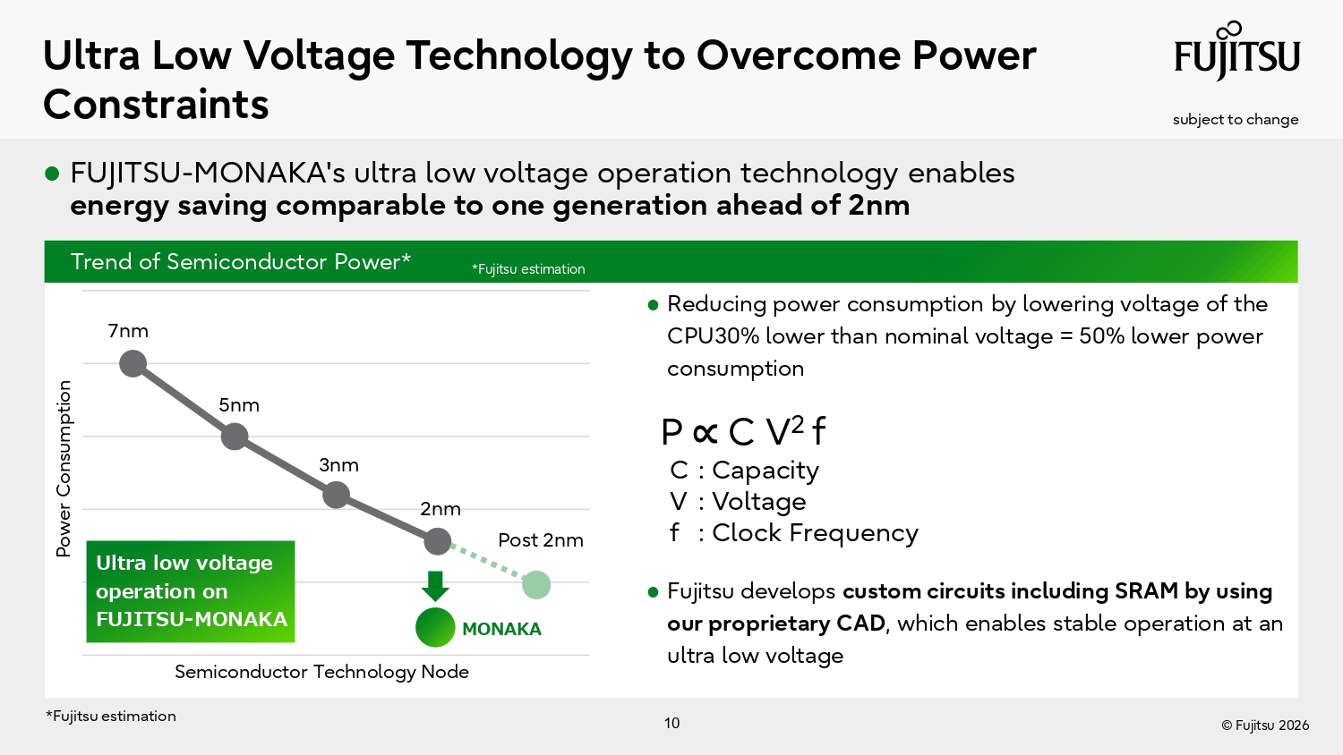
Fujitsu estimates the 350W SKU at 4,355 GFLOPS in DGEMM and 69.7 TOPS in INT8, and the 500W SKU at 6,013 GFLOPS and 96.2 TOPS, with both parts rated around 500 GB/s in STREAM Triad. The company claims up to two-times AI performance and over 50% TCO reduction against unnamed comparisons, and credits ultra-low-voltage operation, running the core around 30% below nominal voltage for roughly half the power, for holding 144 cores inside the 350W envelope. Okazaki described the voltage technique as delivering “energy saving comparable to moving one generation beyond the 2 nanometers,” achieved with custom SRAM and a proprietary CAD flow tuned for non-standard low-voltage operation.
By 2027, Monaka’s 144 cores will land in the middle of the Arm server field rather than at the top of it. AWS’s Graviton5 reaches 192 Neoverse V3 cores on a single 3nm die, Ampere’s roadmap runs to 512 cores in AmpereOne Aurora, and Microsoft‘s Cobalt 200 packs 132 cores with its own per-core DVFS. Monaka’s separation from that group rests on the cache-on-die stack and 12-channel DDR5 bandwidth rather than core count, and its 256-bit SVE2 width matches SiPearl’s Rhea1 while exceeding the 128-bit SVE2 common to hyperscaler Arm cores.
NEDO subsidizes Monaka under a green data center program targeting 40% energy savings by 2030, yet the chip’s 2nm and 5nm dies come from TSMC rather than a domestic fab. That gap between a made-in-Japan design and Taiwanese manufacturing sits awkwardly against the sovereignty that Fujitsu and RIKEN are seemingly keen to attach to the program.
Japan has committed more than 2 trillion yen to Rapidus for 2nm production in Hokkaido by 2027, and roughly 1.2 trillion yen to TSMC’s Kumamoto fabs, and NEDO has separately backed a dedicated 1.4nm AI chip from Fujitsu and IBM Japan to be built entirely in Japan by Rapidus. Monaka predates that domestic capacity, however.
Monaka’s successor is already assigned to a flagship machine. FugakuNEXT, the roughly $750 million RIKEN system announced in August last year with Fujitsu and Nvidia, will pair a 1.4nm-class Monaka-X that adds Arm SME2 with Nvidia GPUs linked over NVLink Fusion, the interconnect Nvidia opened to third-party CPUs in 2025. RIKEN targets more than 600 FP8 exaFLOPS within a 40MW envelope and roughly 100 times Fugaku’s application performance, with operation around 2030. FugakuNEXT is Japan’s first flagship supercomputer to place GPUs at its core, a departure from the CPU-only A64FX design of the original Fugaku.
Fujitsu has firmed up rather than changed the Monaka plan across three years of disclosures, with the core count, node split, and an anticipated launch date of 2027 remaining unchanged since 2023. Fujitsu didn’t disclose pricing, and its DGEMM, STREAM, and INT8 figures remain estimates until independent testing at the 2027 launch
Full Fujitsu Monaka Hot Chips 2026 presentation